Sputtering
Sputtering System & Equipment
Table of contents
- Sputtering deposition systems & sputtering equipment
- What is sputtering?
- When to choose sputtering deposition
- Sputtering overview
- Step-by-step buying guide
- Typical applications for sputtering
- Why buy sputtering equipment from us
Sputtering deposition systems & sputtering equipment
TL;DR: A sputtering system ejects atoms from a target in a controlled plasma, then deposits a dense, uniform thin film on the substrate. It delivers tight uniformity, stable rates, and excellent adhesion at low to moderate temperatures. Use sputtering deposition when you need production-grade films on wafers, glass, metals, or polymers with repeatable results.
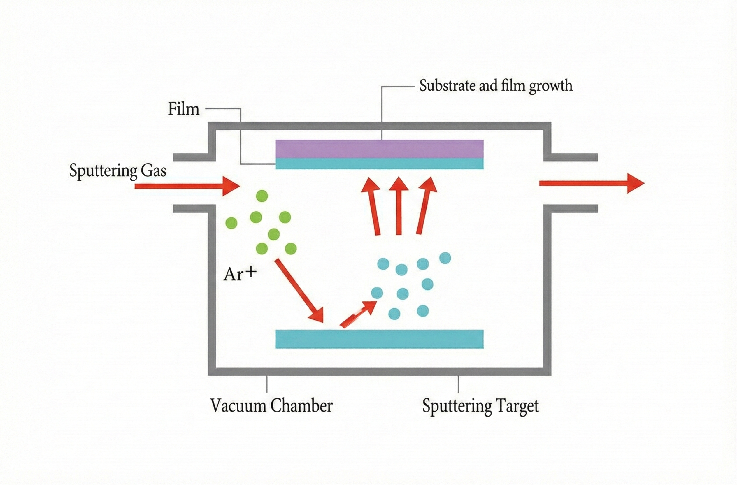
What is sputtering?
Sputtering is a physical vapor deposition process that accelerates ions in a low-pressure gas to knock target atoms into the gas phase, which then condenses on the substrate. It produces dense films with good step coverage and precise thickness control. Compared with evaporation, sputtered layers are usually denser and more uniform at similar temperature budgets.
Benefits in one look:
- Dense films, excellent uniformity and adhesion
- Low to moderate substrate temperature, suitable for polymers and wafers
- Reactive runs for oxides and nitrides, multi-target stacks possible
- Scales from R&D to 200/300 mm production with automation
When to choose sputtering deposition?
Choose sputtering equipment if you need:
- Uniform metallic or ceramic films with tight tolerances
- Reactive oxides or nitrides such as SiOₓ, SiNₓ, TiN
- Low-temperature processing with robust adhesion
- High repeatability for optics, semiconductors, medtech and wear coatings
Sputtering overview
Sputtering is PVD with a plasma that ejects atoms from a target and deposits a dense, uniform thin film on the substrate. A sputtering system achieves high uniformity at low to moderate temperatures. It suits 200/300 mm wafers, glass, metals, and polymers.
Overview table
| Aspect | Answer |
|---|---|
| Process | Sputtering deposition with ion bombardment in vacuum |
| Core effect | Dense films, very good uniformity, strong adhesion |
| Temperature budget | Low to medium, heating available if needed |
| Typical materials | Metals, alloys, oxides and nitrides via reactive sputtering |
| Substrate sizes | Samples up to 200/300 mm plus parts with fixtures |
| Deposition rate | Medium to high, depends on source and target |
| Sources & power | DC or RF, optional magnetron multi-cathode |
| Process control | MFC gas delivery, pressure control, recipe control, QCM or optical monitoring |
| Automation | Load-lock, EFEM/FOUP, production data logging |
| Main uses | Optics and filters, semiconductors, medtech, wear coatings, energy |
Advanced sputtering options
| Option | Purpose | Result |
|---|---|---|
| Magnetron sputtering | Magnetic field increases plasma density | Higher rate, very dense films, lower pressure |
| Reactive sputtering | O₂ or N₂ to form compounds | Oxides and nitrides with controlled stoichiometry |
| Pulsed DC / RF | Stabilize insulating or arc-prone targets | Less arcing, smoother films |
| Substrate bias | Control ion energy at the substrate | Densification and stress tuning |
| Planetary motion | Optimize substrate path | Typical ±2–5% uniformity even on complex parts |
Specification snapshot
| Specification | Typical range |
|---|---|
| Base pressure | 1×10⁻⁶ to 1×10⁻⁸ mbar, process at a few mTorr |
| Uniformity | ±2–5% with suitable fixtures and motion |
| Temperature | Room temperature to about 400 °C depending on setup |
| Monitoring | QCM rate, ellipsometry, thickness mapping, SPC |
| Safety | Interlocks, exhaust, gas safety, CE depending on scope |
Step-by-step buying guide
| Step 1 | Define substrate, size, and temperature limit. |
| Step 2 | Set film stack and KPIs such as uniformity and stress. |
| Step 3 | Pick source configuration, magnetron type, and power supplies. |
| Step 4 | Specify gas panel and reactive control for oxides or nitrides. |
| Step 5 | Choose fixtures and motion for coverage and repeatability. |
| Step 6 | Decide on automation and metrology, then lock acceptance tests. |
Typical applications for sputtering
Optical stacks via sputtering
Use sputtering deposition for dense, index-stable AR, HR and BBAR stacks with ±2–3% uniformity and low scatter. Typical sputtered films include TiO₂, SiOₓ/SiNₓ and ITO on glass or polymers. Validate with thickness maps and ellipsometry. Not ideal when fully conformal 3D coverage at very low temperature is mandatory.
Wafer metallization and passivation by sputtering (200 mm and 300 mm)
Choose sputtering for seed, barrier and passivation with clean interfaces and repeatable runs. Common stacks are Ti/TiN, Al, Cu and SiNₓ/SiOₓ in reactive mode. The Production frame includes load lock, EFEM/FOUP, recipe control and SPC with a ±2–5% uniformity target and low particles. Prefer PECVD or ALD only when extreme conformality is the primary constraint.
TiN sputter coatings for medical devices
Apply sputtering equipment for hard, clean and biocompatible films such as TiN or thin barrier layers at low to moderate temperatures. Verify with adhesion testing, contact angle and sterilization stability. Use hybrid routes when specific DLC chemistries are required.
Magnetron sputter hardcoats for wear protection
Magnetron sputtering deposits dense TiN, TiCN and CrN for tools and precision parts with low friction and high hardness. Tune fixtures and optional substrate bias to balance stress and coverage. Prove performance with tape or scratch tests and friction under load.
Sputtered electrodes and barriers for energy and sensors
Select a sputtering system for conductive, catalytic and barrier layers in batteries, fuel cells, PV and sensing. Typical films include ITO or alternatives, Ni/Co and diffusion barriers. Focus on sheet resistance, optical transmission and scale-up from R&D to pilot lines.
Why buy sputtering equipment from us
We size the sputtering system to your process and deliver the surrounding stack, from vacuum and gas delivery to handling and metrology. You receive full documentation and acceptance testing as defined in the project scope, plus ongoing service covering installation, preventive maintenance, repairs and upgrade programs. Our partner ecosystem spans thin-film systems, wafer handling, atmospheric plasma, wet processing (SRD), rapid thermal processing and metrology standards, ensuring compatible interfaces and predictable deployment.
CONTACT US
Novel Technology Transfer GmbH
Dorfstrasse 16
85235 Pfaffenhofen a.d. Glonn
Germany
Phone +49 (0)8134 55700-0
Fax +49 (0)8134 55700-10
Mail info@novel-tec.de


REQUEST A CALL