Thin Film
Thin Film Deposition
Table of contents
- What is thin film? Core concepts & use case
- Thin film deposition methods at a glance
- Thin film deposition system overview
- Thin film coating equipment vs thin film process equipment
- How to choose the right thin film technology
- Thin film system supplier & integration partners
- Applications & industries for thin film deposition
What is thin film? Core concepts & use case
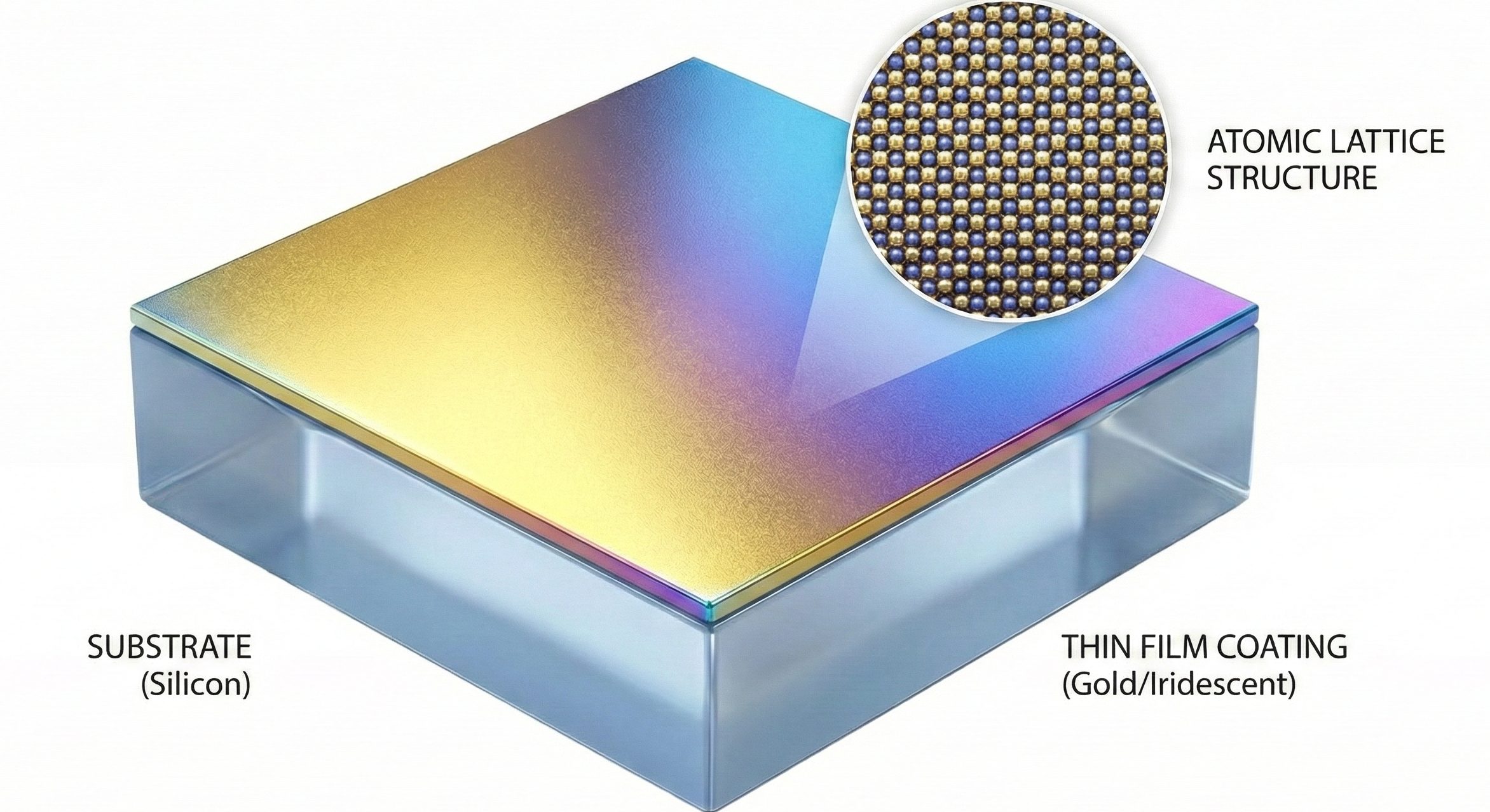
A thin film is a functional layer with a thickness typically from a few nanometers up to a few micrometers that is deposited onto a substrate to tailor optical, electrical, mechanical, or chemical properties. Unlike bulk materials, performance is dominated by the interface (film–substrate), the film’s microstructure (density, grain size, stress), and the thickness itself. Typical substrates include silicon wafers (200/300 mm), glass, metals, and polymers.
Key concepts in thin film technology:
- Deposition method: e.g., PVD (sputtering, magnetron), electron-beam or thermal evaporation, and PECVD -
each with different temperature budgets, rates, and uniformity. - Uniformity & thickness control: across the wafer/part; critical for
device yield and optical performance. - Adhesion & surface preparation: pre-clean/activation (e.g., plasma) to ensure
robust bonding and coating adhesion. - Metrology: thickness mapping, refractive index, sheet resistance, roughness, and adhesion tests.
Representative use cases:
- Optics & photonics: AR/HR/BBAR stacks, interference filters.
- Semiconductor & MEMS: barrier/seed layers, interconnects, passivation.
- Medical & wear protection: DLC and other hard, low-friction coatings.
- Energy & sensors: transparent conductors, catalytic and protective layers.
This foundation frames the selection of a thin film deposition method and the right thin film equipment for each application.
Thin film deposition methods at a glance
The choice of deposition method depends on the material, temperature budget, film density/uniformity, and throughput. Here’s the overview:
| Method | Temp. budget | Deposition rate | Film density/ uniformity | Typical films / use | Notes |
|---|---|---|---|---|---|
| PVD (overview) | Low to mid | Mid | Good | Metals, alloys | Umbrella for evaporation/sputtering methods |
| Sputtering | Low to mid | Mid | Very good (dense films, strong step coverage) | Metals (Al, Cu, Ti, W), oxides/nitrides (ITO, SiOx, SiNx, TiN) | Reactive sputtering for compounds |
| Magnetron sputtering | Low to mid | Mid to high | Very good | As sputtering, with higher throughput (large areas, hard coatings) | Magnetic confinement -> higher rates, stable windows |
| Electron-beam evaporation | Low (minimal substrate heating) | High | Good (directional; rotation/fixturing recommended) | Noble/high-purity metals | Very high rates; line-of-sight |
| Thermal evaporation | Low | Mid | Good | Metals and organics (moderate melting points) | Simple hardware; great for prototyping/optics; material-dependent |
| PECVD (plasma-enhanced CVD) | Low (low-temperature growth) | Mid | Good, chemistry-tunable | SiOx, SiNx, a-Si:H, selected DLC/barrier/passivation layers | Plasma-assisted, gas-phase; conformal films at low temp |
Thin film deposition system overview
A thin film deposition system combines vacuum hardware, deposition sources, controlled motion/fixturing, and precise process control, optionally with automated wafer handling for 200/300 mm. The goal is repeatable films at target thickness, uniformity, and throughput, with clean chemistry and stable pressure/power windows. Many setups are built as integrated platforms where chamber design, source configuration, and automation interfaces are defined as a system concept, as seen in INTLVAC platform families. This section outlines the core building blocks and a quick spec snapshot for selection.
Core components:
- Vacuum stack: chambers, dry/turbo pumps, throttled pressure control; optional load-lock.
- Sources & power: sputtering (DC/RF/magnetron), evaporation (e-beam, thermal), reactive gas options.
- Motion & fixturing: rotation/planetary, heating/cooling, masking, carriers for wafers, glass, metals, polymers.
- Process control: MFCs (mass flow controllers), pressure control, power matching, recipe logic, QCM/optical monitoring.
- Handling & interfaces: EFEM/FOUP, load ports, cassettes, vacuum transfer to cluster tools.
- Metrology & safety: thickness/uniformity mapping, ellipsometry, sheet resistance; interlocks, exhaust/scrubbers.
Spec snapshot
| Spec point | Typical range / note |
|---|---|
| Wafer/part size | Up to 200/300 mm (fixtures for parts/glass) |
| Base pressure | 1×10⁻⁶ – 1×10⁻⁸ mbar (method-dependent) |
| Temperature budget | Room temp to ~400 °C (options available) |
| Deposition rate bands | Sputtering: mid · E-beam: high · Thermal/PECVD: mid |
| Film uniformity (typ.) | ±2–5 % across substrate (fixture/process dependent) |
| Automation options | Load-lock, EFEM/FOUP, vacuum transfer/cluster integration |
Thin film coating equipment vs thin film process equipment
Thin film coating equipment is the deposition tool that forms the film on the substrate. Thin film process equipment comprises the supporting stack, including vacuum pumps and a load-lock, gas delivery (MFCs), power and cooling, handling (EFEM/FOUP), metrology, exhaust and safety systems, which keeps chemistry, pressure and power stable for repeatable thickness, uniformity and throughput. In practice buyers assess both together: the coater for capability, and the process stack for yield and uptime.
| Aspect | Thin film coating equipment | Thin film process equipment |
|---|---|---|
| Primary role | Creates the film (PVD/evap/PECVD) | Enables stable, safe, repeatable processing |
| Typical scope | Chamber, sources (sputter cathodes, e-beam/thermal), fixtures, heaters/cooling | Vacuum pumps & load-lock, gas lines/MFCs, power/cooling, EFEM/FOUP handling, metrology, exhaust/safety |
| Key KPIs | Rate, uniformity, film properties | Base pressure, gas/pressure stability, uptime, contamination control |
| Buying trigger | New method/capability, higher deposition rate, larger substrates | Yield drift, base-pressure or contamination limits, scaling to 200/300 mm |
| Example items | Magnetron sputter tool, e-beam evaporator, thermal evaporator | Turbos/dry pumps, load-lock, MFC gas panel, chiller, EFEM/FOUP, QCM/ellipsometry, scrubber |
| Integration | Tool-level recipes, motion/fixtures | Plant-level reliability (SPC), interlocks, data logging, maintenance routines |
How to choose the right thin film technology
Choosing the right thin film technology depends on temperature budget, film type, uniformity needs, substrate sensitivity and throughput. Use the matrix below to narrow options, then jump to the spoke pages for detailed specs.
| Criterion | Sputtering | Magnetron sputtering | E-beam evaporation | Thermal evaporation | PECVD |
|---|---|---|---|---|---|
| Low substrate temperature | ✓ | ✓ | ✓✓ | ✓✓ | ✓✓ |
| Highest deposition rate (metals) | ✓ | ✓ | ✓✓ | ✓ | – |
| Dense films & top uniformity | ✓✓ | ✓✓ | ✓ | ✓ | ✓ |
| Complex shapes / better step coverage | ✓✓ | ✓✓ | – | – | ✓✓ |
| Reactive/compound films (oxides/nitrides) | ✓✓ | ✓✓ | – | – | – |
| Very high purity / noble metals | ✓ | ✓ | ✓✓ | ✓ | – |
| Large-area productivity | ✓ | ✓✓ | ✓ | – | ✓ |
| Conformal films at low temp | – | – | – | – | ✓✓ |
| Capex simplicity / quick prototyping | ✓ | ✓ | – | ✓✓ | ✓ |
How to read it
- Start with non-negotiables (e.g., low temp + dense film + complex geometry).
- Pick the method with most ✓✓ and fewest –, then verify on the spoke page (materials, size, rate).
Quick decision cues
- Need the highest metal rate with minimal heating → E-beam.
- Need dense, uniform metallic/ceramic films or reactive oxides/nitrides → (Magnetron) sputtering.
- Need conformal films at low temperature with chemistry control → PECVD.
- Need simple, gentle lab setup or optics prototyping → Thermal evaporation.
Thin film system supplier & integration partners
As a thin film system supplier and integrator, we match the method to the job and deliver the complete stack around it: vacuum with load-lock, sources and power, motion and fixtures, gas delivery (mass flow controllers, MFCs), handling (EFEM and FOUP), metrology, and safety. We work with established brands such as Intlvac for thin film systems, Hine for automation including wafer handlers and load modules, Surfx for atmospheric plasma, HF Semi for wet processing and spin rinse dryers (SRD), SSI for rapid thermal processing (RTP/RTA), and AP Applied Physics for metrology and standards.
Projects follow a clear path from requirements and design review to factory and site acceptance as defined in the project scope. You receive complete documentation, including P&IDs, schematics, and recipes, and tested performance against agreed targets such as ±2–5% uniformity, along with safety concepts with interlocks and exhaust. After handover, we support you with preventive maintenance and calibration, spare parts and upgrades (for example cathodes, e-beam guns, load-lock modules, EFEM kits), remote assistance, and SLAs.
Applications & industries for thin film deposition
Optics & filters - thin film deposition for optical stacks
Deliver uniform AR/HR/BBAR stacks and edge-sharp filters with stable refractive index control.
- Typical films: SiOₓ / SiNₓ, TiO₂, Al₂O₃, ITO
- KPIs: thickness tolerance ±2–3%, low scatter/defectivity
- Use cases: AR on glass/polymer, interference filters, mirrors
Semiconductors - thin film deposition for wafers (200/300 mm)
Repeatable seed/barrier/passivation layers with clean interfaces and tight within-wafer uniformity.
- Typical films: Al, Cu, Ti/TiN, SiOₓ/SiNₓ
- Process context: load-lock, EFEM/FOUP, recipe control, SPC
- KPIs: uniformity ±2–5%, low particles, high uptime
MedTech & life sciences - biocompatible thin films
Hard, low-friction and biocompatible coatings for implants, instruments and diagnostics.
- Typical films: DLC (a-C:H/ta-C), TiN, SiOₓ barrier
- Benefits: wear resistance, corrosion control, cleanability
- Validation: contact angle, cytotoxicity, sterilization stability
Wear-resistant coatings - durability & low friction
Dense, adherent layers for tooling, automotive and precision mechanics.
- Typical films: DLC, TiN/TiCN, CrN
- KPIs: hardness, coefficient of friction, adhesion (tape/scratch)
- Geometry: rotation/planetary fixturing for coverage
Energy & sensors - functional thin films
Conductive, catalytic and protective layers for batteries, fuel cells, PV and sensing.
- Typical films: ITO/ITO-alternatives, Ni/Co, barrier and catalyst layers
- Focus: sheet resistance, optical transmission, stability
- Scaling: from R&D to pilot lines
CONTACT US
Novel Technology Transfer GmbH
Dorfstrasse 16
85235 Pfaffenhofen a.d. Glonn
Germany
Phone +49 (0)8134 55700-0
Fax +49 (0)8134 55700-10
Mail info@novel-tec.de


REQUEST A CALL