Physical Vapor Deposition
PVD Technology & Applications
Table of contents
- PVD coating systems
- What is physical vapor deposition?
- Why choose PVD for your application?
- PVD process overview
- System portfolio & key specifications
- Application of PVD technology
- PVD technologies we deliver
PVD coating systems
Physical vapor deposition (PVD) is a vacuum-based coating process used to create high-quality thin films on wafers and precision components. With our dedicated PVD coating systems, we support customers in semiconductors, optics and advanced manufacturing who need stable processes, tight film uniformity and reliable adhesion. Novel Tec acts as an integration partner for PVD technology, combining process know-how, hardware and automation into complete solutions. We help you select and configure the right PVD deposition system for your substrate sizes, materials and throughput targets, and support you from first trials through to qualified production.
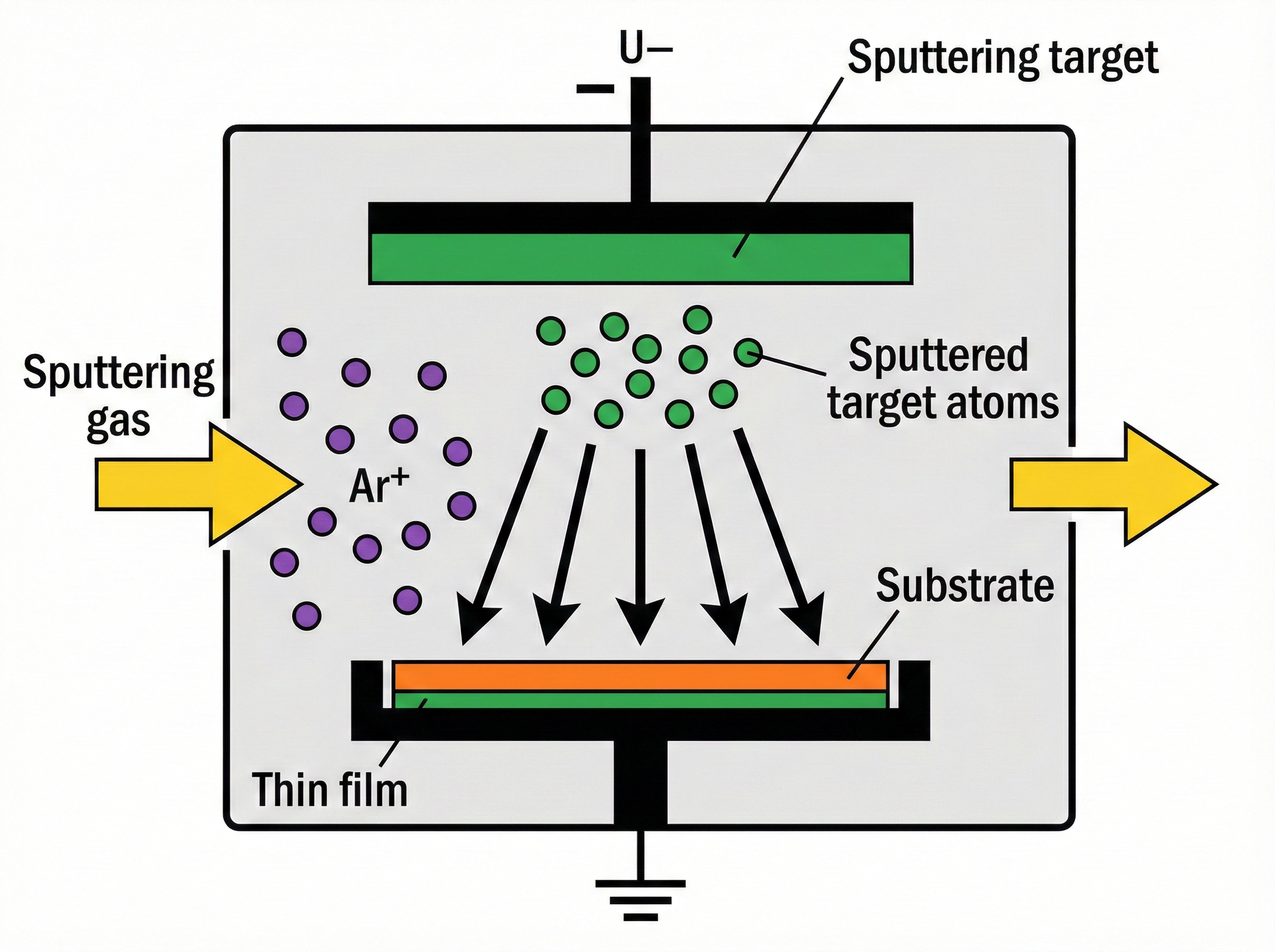
What is physical vapor deposition?
Physical vapor deposition transfers material from a solid source to a substrate in several controlled steps. Energy is applied to a target, atoms are knocked out or evaporated, move through a low-pressure gas and condense as a thin film on the surface. The process is mainly line-of-sight, which makes it well suited for precise, directional coatings. The core principles of a stable PVD process are constant vacuum conditions, controlled energy input and repeatable substrate handling. Key parameters include base pressure, process gas composition, power, substrate temperature and time. By adjusting these variables, engineers tailor film thickness, microstructure, stress, adhesion and electrical or optical properties. Compared to wet plating or painting, PVD uses solid sources and clean vacuum environments to achieve highly reproducible coatings with low contamination.
Why choose PVD for your application?
Choosing PVD for your application gives you a combination of film quality, flexibility and process control that many other coating methods cannot offer:
- High quality thin films: Achieve tight thickness and uniformity control on wafers and complex parts, with stable PVD processes that are easy to repeat and scale.
- Wide material and stack options: Deposit metals, alloys and compounds in single layers or multilayer stacks using one PVD coating system, from barrier and seed layers to functional and decorative films.
- Strong adhesion and durability: Combine proper surface preparation with optimised PVD treatment to get coatings that adhere well and withstand thermal, mechanical and chemical stress.
- Clean, dry and production-friendly: Work in a vacuum with solid sources instead of wet chemistry, reducing contamination risks, waste handling and line complexity.
- Scalable equipment concepts: Start with development tools and move to high-throughput PVD equipment using similar recipes, interfaces and automation.
PVD process overview
The PVD process in production runs through a few repeatable steps:
| Step 1 | Parts or wafers are loaded into the chamber or load lock, and the system is pumped down to the required base pressure. |
| Step 2 | If needed, a pre-clean or plasma activation step prepares the surface for good adhesion. |
| Step 3 | Process gases and power are set, the plasma or evaporation source is started, and the conditions in the chamber are stabilised. |
| Step 4 | Material from the target is transferred through the vacuum and condenses as a thin film on the substrates until the programmed thickness is reached. |
| Step 5 | The system cools if required, then vents and unloads the coated parts for inspection or the next process step. |
System portfolio & key specifications
Our PVD coating systems are configured to match your process window rather than forcing you into a fixed product family. Each project starts from a proven platform and is adapted to wafer size, materials, throughput and integration level. The table below summarises the typical capability ranges and key parameters we can achieve with a customised PVD deposition system.
| Feature | Typical capability range | Configuration examples |
|---|---|---|
| Substrate handling | Wafers up to 300 mm, small parts, carriers & panels | Single wafers, batch carriers, frames, custom fixtures |
| Materials | Metals, alloys, nitrides, oxides, carbon-based layers | Al, Cu, Ti, TiN, Cr, Au, barrier/seed, DLC |
| PVD methods | Magnetron sputtering, co-sputtering, optional evaporation | DC/RF sputtering, reactive sputtering, multi-cathode setups |
| Chamber concept | Single or multi-chamber, with or without load-lock | Standalone process chamber, load-lock tool, cluster integration |
| Deposition rate | From sub-nm/min to several µm/hr | Optimised for uniformity, step coverage or throughput |
| Thickness uniformity | Down to ±1.5 % on supported wafer sizes | Recipe and hardware tuning for critical layers |
| Base pressure | High and ultra-high vacuum regimes | Typical process base pressure < 5 × 10^-7 mbar |
| Automation | Manual to fully automated | Cassette loaders, EFEM, vacuum wafer handler, factory interface |
| Cleanroom compatibility | Integration into ISO 6 to ISO 5 environments | Side-by-side with existing thin film and metrology tools |
Application of PVD technology
PVD technology is used across a wide range of high-tech industries, each relying on specific deposition methods to meet its performance and reliability targets. The table below gives an overview of key sectors and the typical PVD methods and applications in each.
| Industry | PVD Methods Used | Applications |
|---|---|---|
| Semiconductors | Magnetron Sputtering, Co-sputtering, E-beam | Wafer coating, MEMS, Thin-film deposition |
| Automotive | Magnetron Sputtering, Ion Plating | Engine parts, Coatings for wear resistance |
| Aerospace | Magnetron Sputtering, Ion Beam Deposition | Aerospace components, Surface activation |
| Medical Devices | Magnetron Sputtering, PECVD | Biocompatible coatings, Medical equipment |
| Optics | Magnetron Sputtering, E-beam, Co-sputtering | Anti-reflective coatings, Optical lenses |
| Tooling & Industrial | Sputtering, Ion Plating | Cutting tools, Wear-resistant coatings |
| Solar Panels | Magnetron Sputtering, PECVD | Thin-film solar cells, Transparent coatings |
PVD technologies we deliver
At Novel Tec, the focus is on PVD solutions that provide a stable, repeatable process window for thin film deposition. Each PVD coating system is configured around suitable components, chamber concepts and recipes so that uniformity, adhesion and throughput can be matched to the customer’s requirements. To build trust, we communicate target specifications up front and review them together during trials and acceptance. Customers work directly with engineers who understand both the PVD process and the integration of the equipment into existing production lines, including handling, metrology, and service concepts.
CONTACT US
Novel Technology Transfer GmbH
Dorfstrasse 16
85235 Pfaffenhofen a.d. Glonn
Germany
Phone +49 (0)8134 55700-0
Fax +49 (0)8134 55700-10
Mail info@novel-tec.de


REQUEST A CALL